If you want to understand why Europe is pouring hundreds of millions of euros into semiconductor research, you need to grapple with a number that Jean-René Lèquepeys, the deputy director and CTO of CEA-Leti, likes to cite.
The semiconductor industry itself is worth roughly $600 billion globally. But the digital economy it enables is worth about $16 trillion. That's roughly 15-16% of global GDP.
"It is a big enabling technology and a sovereignty technology," Lèquepeys said in an interview.
The problem is that Europe once commanded 30 percent of global chip manufacturing. Today, that figure has cratered to between 5 and 7 percent, even as demand for semiconductors has exploded across every sector from automotive to healthcare to defense. The continent finds itself dangerously dependent on Asian foundries and American design houses for the very components that power its economy, its military systems, and increasingly its AI ambitions.
France, home to heavyweights like STMicroelectronics and Soitec, has positioned itself as a leader in Europe's push to claw back some of that lost ground. Both companies have a large presence in Grenoble and have long partnered with CEA-Leti, making the southern French city a natural home for a semiconductor pilot line at the heart of an €830 million program co-funded by the European Commission under the Chips Act.
The FAMES inauguration only reinforces Grenoble's status as one of Europe's premier semiconductor hubs. CEA-Leti's total cleanroom space now stands at 14,000 square meters, and combined with STMicroelectronics' massive fab in nearby Crolles and a growing ecosystem of startups and research institutions, the region's gravitational pull continues to grow.
But the pilot line isn't just about advancing technology in a lab. It's about proving that Europe can still turn world-class research into industrial-grade capability before someone else eats its lunch. This public-private collaboration has also been a core characteristic of the Grenoble ecosystem, and the project hopes to leverage this mindset to demonstrate.
"Something fails in the equation because we do not manage to transform very smart ideas, good ideas, into manufacturing capacity," Lèquepeys said.
And so, the stakes are hard to overstate
Not a Future Promise
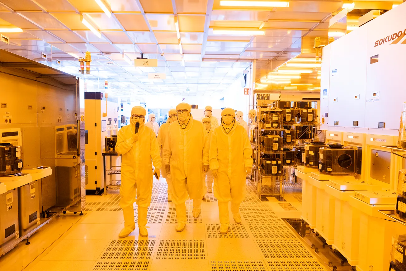
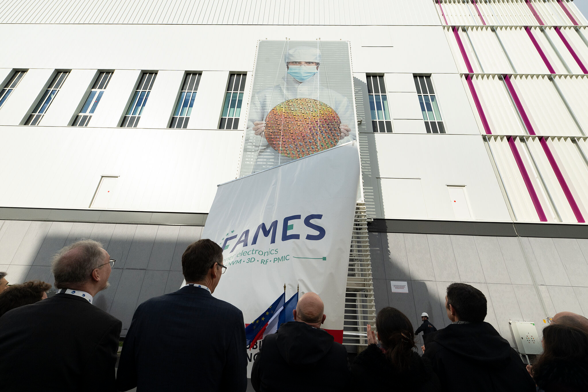
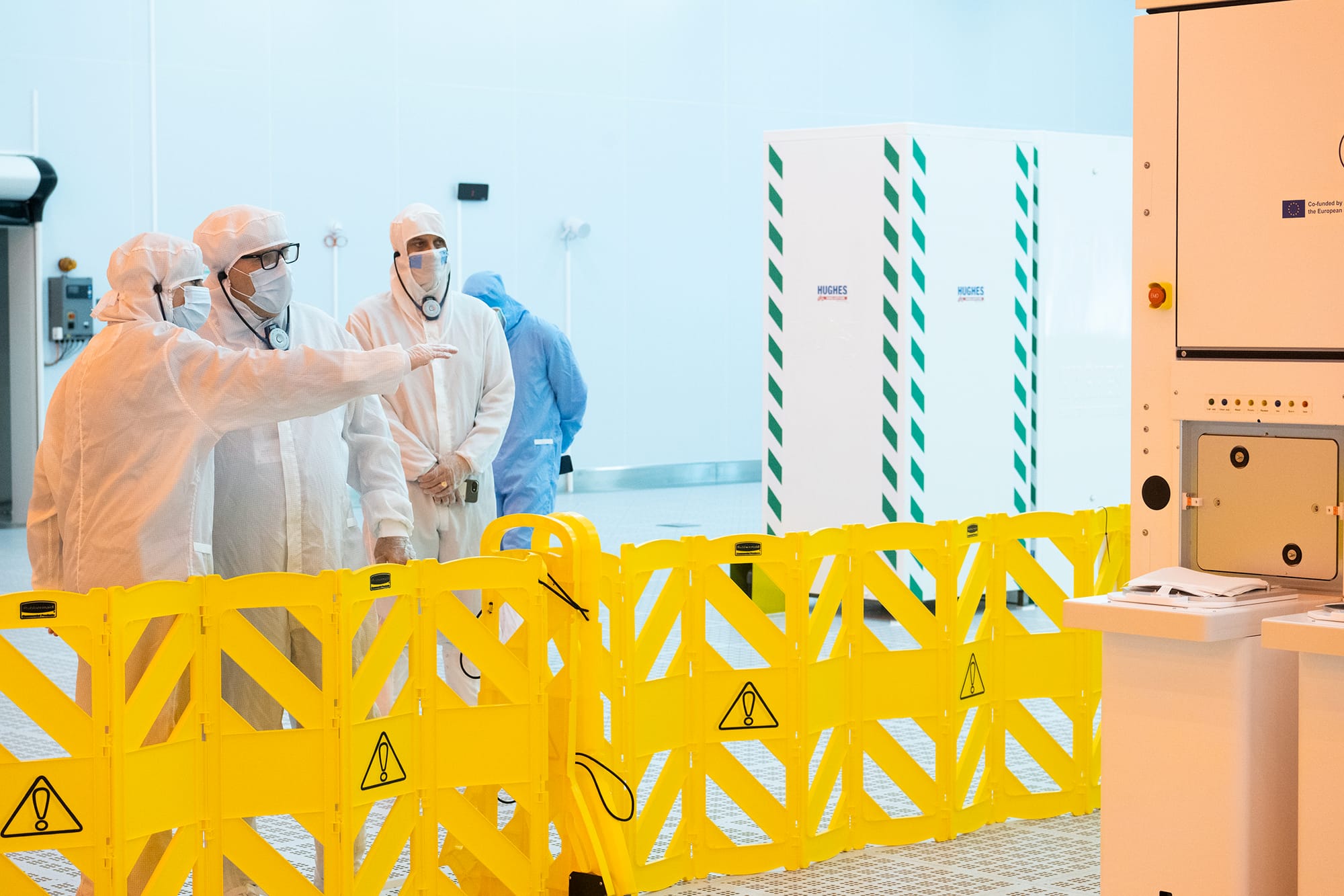
Which is why the official inauguration on January 30 in Grenoble was more than a typical ribbon-cutting ceremony. More than 350 people gathered at CEA-Leti's campus to mark the opening of a new 2,000-square-meter cleanroom extension, a facility designed to house more than 80 state-of-the-art 300mm tools, including space for ASML EUV lithography machines.
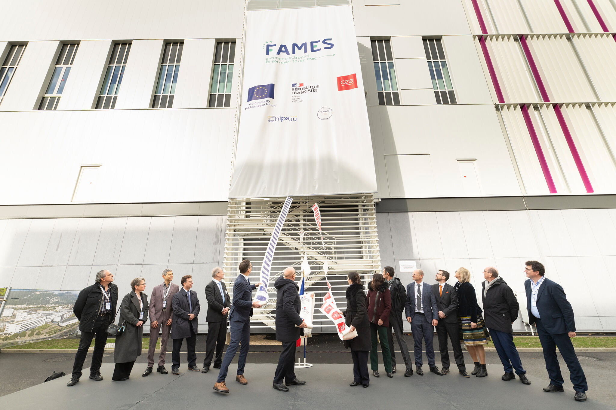
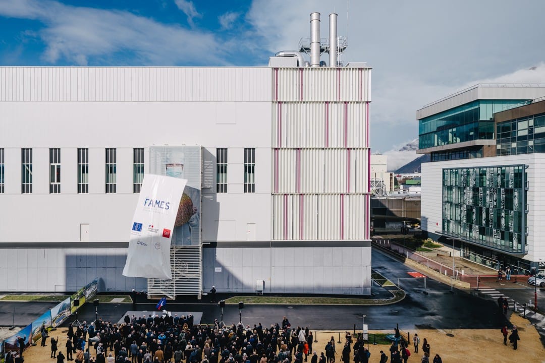
Photos courtesy of CEA-Leti
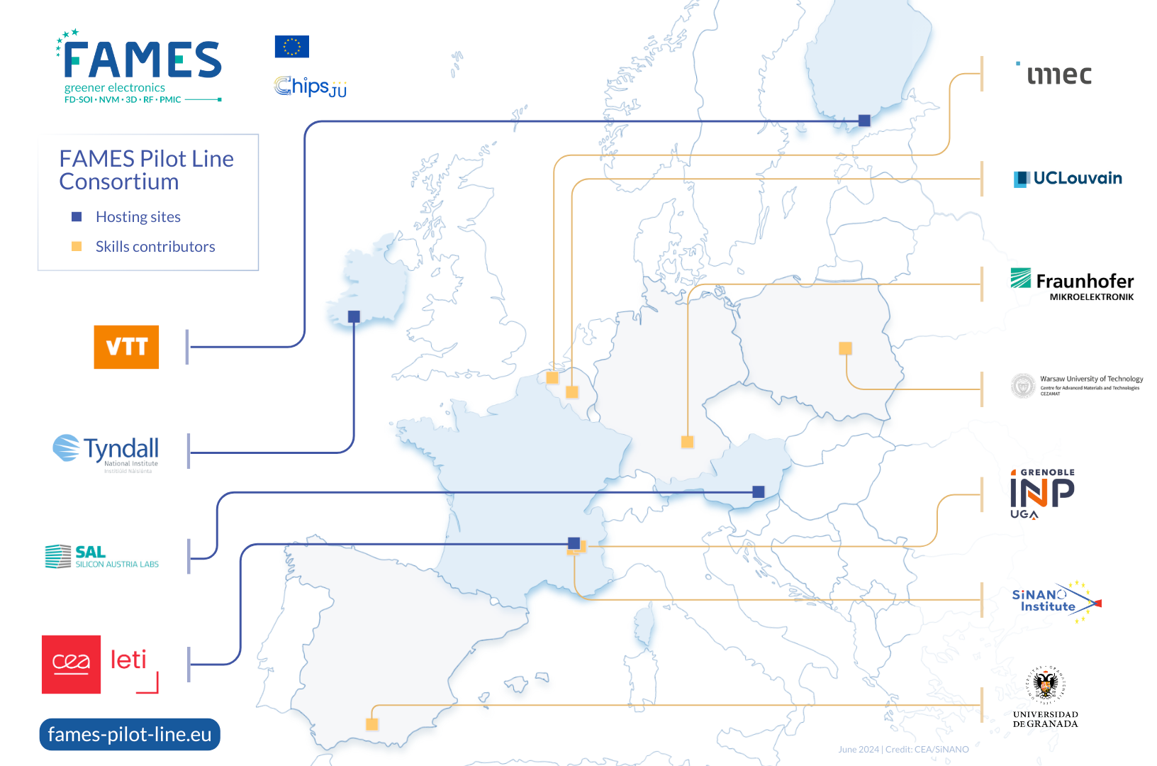
The FAMES Pilot Line is short for "FD-SOI Pilot Line for Applications with embedded non-volatile Memories, RF, 3D Integration & PMIC, to ensure European Sovereignty."
The pilot line brings together 11 partners across eight countries, with CEA-Leti as coordinator. Its open-access model means European startups, SMEs, industrial groups, and research organizations can use the facility to prototype, qualify, and de-risk advanced semiconductor technologies before committing to industrial deployment. Some 44 industry stakeholders already support the initiative, including Nokia, Ericsson, Stellantis, Intel, Meta, STMicroelectronics, GlobalFoundries, and Soitec.
The technology at the heart of FAMES is FD-SOI, or Fully Depleted Silicon-on-Insulator. That's a semiconductor architecture developed by CEA-Leti that simplifies the manufacturing process while delivering strong performance in power consumption, density, speed, and RF behavior.
It's already in production at Samsung, GlobalFoundries, and STMicroelectronics, with much of that production happening in Europe — in Crolles, France, and Dresden, Germany.
FAMES aims to push it to 10nm and 7nm nodes.
To put that in plain terms: shrinking transistors to smaller nodes means you can pack more of them onto a chip, which translates directly into faster processing, lower power consumption, and smaller, cheaper components.
The current generation of FD-SOI chips at 18nm and 22nm is already powering everything from connected cars to IoT sensors. Getting to 10nm and 7nm would represent a massive leap, opening the door to chips sophisticated enough to run AI workloads at the edge, meaning directly on a device rather than sending data to a distant, energy-guzzling data center.
Edge AI is expected to be one of the fastest-growing segments in semiconductors, and it plays to FD-SOI's strengths: low power, high performance, and the ability to integrate digital, analog, and radio-frequency functions on a single chip.
Europe may not be able to beat NVIDIA. But the goal of the FAMES pilot is to help it be more competitive for the next emerging market.
In that respect, the early signs are at least positive.
The pilot line is already operational. Results have been published and validated at leading international conferences, including IEDM 2025, where CEA-Leti presented fully functional 2.5V SOI CMOS devices fabricated at a thermal budget of 400°C, a breakthrough removing a key barrier to large-scale 3D sequential integration.
Video courtesy of CEA-Leti
The pilot line is developing five sets of technologies beyond FD-SOI:
- embedded non-volatile memories
- radiofrequency components
- two 3D integration options
- small inductances for power management.
The goal is to combine them into disruptive system-on-chip architectures.
"We don't target data center GPU chips," Lèquepeys said, "but our solutions are perfectly suited for edge AI solutions, a very promising market."
Five years from now, FAMES will be measured by technology transfers, licensing deals, and the number of startups created. The project has already passed its first European Commission audit with high marks, meeting all milestones on schedule.
The facility itself was designed for the next 20 to 30 years of semiconductor research, with infrastructure to support equipment that current cleanrooms simply can't accommodate.
FAMES also has a training mission, developing programs at the Master's and PhD levels. That matters because, as Lèquepeys said, attracting top talent in fields like AI is genuinely difficult when competing against salaries at Meta, Google, or IBM.
The Geopolitical Acceleration
If the technical ambitions of FAMES are impressive, the geopolitical context has shifted dramatically since its launch.
The pilot line began in 2023 under the first EU Chips Act, building on France's 2030 NextGen project. But the world has changed fast.
Lèquepeys acknowledged that the geopolitical landscape has transformed the program's open-access policy. When FAMES launched, the United States was considered a "like-minded country" whose companies could access the pilot line. That is no longer automatically the case. For partners outside Europe, the consortium now needs approval from the European Commission.
"The situation has drastically and rapidly changed," he said. "Resilience and sovereignty are becoming more and more important."
He described a semiconductor world caught between China and the United States, with Europe in the middle, trying to find its footing between these two major economic powers. India is emerging as a player too, developing its own semiconductor industry," he said.
The Speed Problem
Beyond geopolitics, there's a more fundamental challenge that FAMES is designed to address: speed.
In an industry where developing a new technology can take a decade, and where getting from technology transfer to a first product can take five years, being slow is existentially dangerous.
Lèquepeys pointed to CEA-Leti's transfer of FD-SOI technology to GlobalFoundries in 2017 as instructive. CEA-Leti embedded 25 engineers at GlobalFoundries for two years to help master the technology. Then GlobalFoundries had to build a design platform, find customers, and get through multiple tape-outs. The whole process took years.
This is why CEA-Leti has been pushing a "lab-to-market" methodology. Not just transferring technology to an industrial partner but actively helping that partner master it and develop first products.
It's a two-phase approach: lab-to-industry for the generic technology transfer, then industry-to-market, where CEA-Leti engineers work on-site at the partner's premises.
"We need to go faster, faster, faster," Lèquepeys said. "If we lose time, we lose market opportunities. The business has been taken by someone else, by another technology."


